The Role of 172 nm EUV Lamps in Perovskite Applications
1. Core Characteristics of 172 nm EUV Lamps and Fundamentals of Perovskite Materials
1.1 Key Physical Properties of 172 nm EUV Lamps
The 172 nm excimer lamp (Xe₂* dimer emission) is a typical light source in the vacuum ultraviolet (VUV, λ < 200 nm) band. Its core advantages stem from three characteristics: high photon energy, high monochromaticity, and low thermal effect:
Photon energy exceeding thresholds: The 7.23 eV photon energy can directly cleave primary organic molecular bonds such as C–C (~3.6 eV bond energy) and C–H (~4.3 eV), triggering direct photochemical reactions without photosensitizers;
Efficient radical generation: It can excite the generation of highly reactive oxygen species (ROS) in an oxygen atmosphere, achieving atomic-level surface cleaning and modification with pollutant decomposition efficiency at the ppb level;
Low-temperature cold light source feature: Substrate temperature rise is less than 5 °C during irradiation, avoiding thermal degradation of perovskite materials and adapting to flexible substrates and low-temperature processes;
High uniformity and scalability: Mainstream equipment can achieve uniform irradiation over 43 mm × 43 mm (uniformity < 3%), with a single lamp length up to 2 m, suitable for full scenarios from laboratories to production lines.

1.2 Core Pain Points of Perovskite Materials and Compatibility with 172 nm Lamps
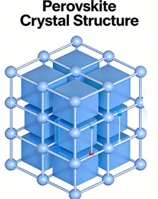
Perovskites (represented by the typical organic–inorganic hybrid perovskite CH₃NH₃PbI₃) have advantages such as high absorption coefficient, long carrier lifetime, and solution processability, but their commercialization bottlenecks focus on three major pain points:
Dense surface defects: Grain boundaries and surfaces contain undercoordinated Pb²⁺, halogen vacancies and other defects, which act as carrier recombination centers and lead to open-circuit voltage (Vₒc) loss;
Interface energy level mismatch: Potential barriers exist at the interface between perovskite and transport layers (e.g., TiO₂, NiOₓ), hindering efficient carrier extraction;
Poor environmental stability: Susceptible to erosion by water, oxygen and ultraviolet light, causing iodide ion migration and crystal structure collapse.
The precise energy transfer and non-contact processing characteristics of 172 nm EUV lamps precisely meet the technical needs to solve the above pain points, making them a key tool for perovskite process upgrading.
2. Four Core Mechanisms of 172 nm EUV Lamps on Perovskites
2.1 Surface Cleaning and Activation: Construction of Atomically Clean Substrates
Mechanism: 172 nm high-energy photons directly cleave organic contaminants (residual precursors, solvent molecules, dust) on the perovskite film surface and substrates (e.g., ITO, glass, polymers), breaking C–C and C–H bonds to form volatile products such as CO₂ and H₂O, achieving damage-free cleaning. Meanwhile, polar functional groups such as hydroxyl (–OH) and carboxyl (–COOH) are introduced on the surface, significantly improving surface hydrophilicity and reactivity.
Quantitative effects:
Contact angle drops from 80° to below 10°, uniformity of perovskite precursor solution spreading improves by 30%, and film coverage increases by 15%–20%;
Surface carbon residue is reduced by more than 90%, eliminating carrier scattering and recombination losses caused by impurities;
Application scenarios: Substrate cleaning before perovskite film preparation and surface activation before precursor coating, especially suitable for low-temperature treatment of flexible substrates (e.g., PI, PET).
2.2 Defect Passivation: Core Pathway to Suppress Non-Radiative Recombination
Mechanism: 172 nm irradiation achieves perovskite defect passivation through two mechanisms:
Vacancy filling effect: High-energy photons excite water molecules in air to decompose into H⁺ and OH⁻; OH⁻ can occupy halogen vacancies (e.g., I⁻, Br⁻), neutralize the positive charge of undercoordinated Pb²⁺, and reduce defect state density;
Lattice repair effect: Photon energy induces slight recrystallization on the perovskite surface, eliminating amorphous phases at grain boundaries and reducing defect concentration.

Key data:
Interface defect state density decreases from 10¹⁵ cm⁻³ to below 10¹³ cm⁻³, close to the theoretical limit;
Carrier lifetime increases from the microsecond level to more than 20 μs, and non-radiative recombination loss is reduced by 40%–60%;
Typical application: Secondary passivation treatment after perovskite film annealing, which can improve the power conversion efficiency (PCE) of perovskite solar cells (PSC) by 10%–20%.
2.3 Crystallization Control: Optimizing Film Microstructure
Mechanism: 172 nm irradiation regulates perovskite crystal growth through photochemically induced crystallization and stress release:
Promotion of low-temperature nucleation: Photon energy stimulates rapid migration of Pb²⁺ and halide ions, lowering the crystal nucleation barrier so that perovskites can complete crystallization at room temperature and avoid phase separation caused by high-temperature processes;
Grain size control: By adjusting irradiation intensity and time, grain size can be increased from 100 nm to over 1 μm, reducing the number of grain boundaries and improving carrier transport efficiency;
Phase structure stabilization: Inhibits phase transition of perovskites from cubic phase (highly light-absorbing) to tetragonal/orthorhombic phase (low activity), maintaining the intrinsic optoelectronic properties of the material.
Experimental verification:
CsPb(Cl/Br)₃ nanocrystals treated with 172 nm light show a 2–3 times increase in grain size and a 15% improvement in crystallinity;
Film roughness decreases from 5 nm to below 1 nm, significantly optimizing surface flatness and reducing carrier scattering.
2.4 Interface Engineering: Optimizing Energy Level Matching and Carrier Extraction
Mechanism: 172 nm irradiation performs precise modification on the perovskite/transport layer interface to solve energy level mismatch:
Energy level alignment optimization: By introducing surface functional groups, the work function of transport layers (e.g., NiOₓ, TiO₂) is adjusted to form a stepwise energy level arrangement between perovskite and transport layers, reducing the carrier extraction barrier;
Enhanced interface bonding strength: Polar functional groups strengthen chemical bonding between perovskite and transport layers, reducing interface delamination and debonding and improving device mechanical stability;
Preparation of dopant-free transport layers: 172 nm irradiation can directly induce the formation of Ni³⁺-rich phases in NiOₓ films, improving hole transport capability without additional doping and simplifying the process flow.
Application results:
In inverted-structure PSCs, NiOₓ hole transport layers treated with 172 nm light increase device PCE from 22.45% to 24.1%, reaching 19.7% for flexible devices;
Interface recombination rate at the perovskite/PCBM interface is reduced by 35%, and fill factor (FF) increases by more than 4%.
3. Typical Application Scenarios of 172 nm EUV Lamps in Perovskite Devices
3.1 Empowerment of the Whole Manufacturing Process of Perovskite Solar Cells (PSC)
表格
| Application Stage | Specific Function | Technical Benefit | Case Data |
|---|---|---|---|
| Substrate pretreatment | Removes organic residues and improves hydrophilicity | Uniform precursor spreading, pinhole-free films | Film coverage +20%, pinhole rate –90% |
| Crystallization control | Low-temperature induced crystallization, optimized grain size | Reduced grain boundary recombination, longer carrier lifetime | Carrier lifetime from 5 μs → 20 μs, PCE +12% |
| Defect passivation | Fills vacancies, repairs lattice defects | Reduced non-radiative recombination, higher Vₒc | Vₒc loss from 110 mV → 56 mV, PCE +20% |
| Interface modification | Adjusts energy level alignment, strengthens interface bonding | Improved carrier extraction efficiency, enhanced stability | FF +4%, 82.8% efficiency retention after 1000 h aging at 85 °C |
| Micro-nano fabrication | Mask-free patterning, direct electrode writing | Enables high-density integration, lower manufacturing cost | Line width down to 0.35 μm, stitching accuracy ±1 μm |
3.2 Performance Upgrading of Perovskite Photodetectors
172 nm irradiation can significantly improve the responsivity and response speed of perovskite ultraviolet photodetectors:
Responsivity increases from 10 A/W to over 40 A/W, detection sensitivity improved by 3 times;
Response time reduced from milliseconds to microseconds (e.g., 8 μs), suitable for high-speed optical communication;
Application scenarios: Deep UV detection, space environment monitoring, flame detection, etc., solving the problems of weak UV response and high cost of traditional silicon-based detectors.
3.3 Key Process Support for Perovskite/Silicon Tandem Solar Cells
Tandem cells are the core direction to break the efficiency limit of single-junction cells. The roles of 172 nm EUV lamps include:
Perovskite top cell preparation: Low-temperature crystallization process avoids high-temperature damage to silicon bottom cells, enabling integration below 200 °C;
Interface passivation: Treats the perovskite/silicon interface to eliminate recombination losses caused by lattice mismatch, with tandem cell PCE exceeding 29%;
Anti-reflection layer fabrication: Directly prepares micro-nano structured anti-reflection layers on perovskite surfaces, improving light absorption efficiency by more than 10%.
3.4 Repair and Performance Regeneration of Degraded Perovskite Devices
Innovative application: 172 nm high-energy irradiation can perform non-destructive repair on degraded PSCs:
Repair mechanism: Photon energy induces re-migration of iodide ions and defect passivation in degraded regions, restoring crystal structure;
Repair effect: Degraded device PCE can be fully recovered, with a 5%–10% improvement over the initial state, while reducing hysteresis;
Application value: Significantly reduces yield loss in perovskite device manufacturing and improves production line economic benefits.
4. Performance Comparison Between 172 nm EUV Lamps and Conventional UV Light Sources
| Performance Indicator | 172 nm EUV Lamp | Conventional 254 nm UV Lamp | Conventional 365 nm UV Lamp |
|---|---|---|---|
| Photon energy | 7.23 eV | 4.88 eV | 3.40 eV |
| Bond cleavage capability | Directly cleaves C–C/C–H bonds | Requires photosensitizer mediation | Only triggers weak photochemical reactions |
| Cleaning efficiency | Atomic-level cleanliness, completed within 10 s | Takes minutes, high residue | Low efficiency, prone to thermal damage |
| Thermal effect | Low temperature (ΔT < 5 °C) | Medium temperature (ΔT < 20 °C) | High temperature (ΔT > 30 °C) |
| Compatible substrates | Flexible / brittle substrates | Mainly brittle substrates | Only high-temperature-resistant substrates |
| Process cost | Lamp lifetime > 5000 h, low energy consumption | Short lifetime, high energy consumption | High energy consumption, low efficiency |
Core conclusion: 172 nm EUV lamps have significant advantages in energy efficiency, process temperature and compatibility, especially suitable for precise processing of heat-sensitive materials such as perovskites.
5. Industrialization Challenges and Solutions
5.1 Core Challenges
Equipment cost and scale-up: Initial investment in 172 nm excimer lamp equipment is relatively high, and production line integration needs to adapt to existing perovskite coating and annealing lines;
Process parameter standardization: Irradiation intensity, time, atmosphere (air/nitrogen) and other parameters significantly affect perovskite performance, requiring a standardized process window;
Long-term stability risks: 172 nm irradiation may induce long-term migration of surface functional groups in perovskites, requiring optimized process parameters to avoid performance degradation.
5.2 Solutions
Domestic equipment and cost optimization: Domestic manufacturers have launched mass-produced 172 nm lamp equipment, with single-lamp costs reduced by 40% compared with imported products, suitable for 500 MW/year production line integration;
Construction of process parameter database: Establish 172 nm irradiation parameter libraries for different perovskite systems (e.g., MAPbI₃, FAPbI₃, CsPbBr₃) through orthogonal experiments to guide production line parameter settings;
Composite process synergy: Combined use of 172 nm irradiation with molecular passivation (e.g., ammonium ligands) and ion doping improves initial performance and long-term stability, avoiding limitations of single processes.
6. Future Development Trends and Prospects
6.1 Technology Upgrading Directions
Multi-light source collaborative application: Combination of 172 nm lamps with infrared and visible light sources to achieve gradient crystallization of perovskite films, further improving grain uniformity;
Breakthrough in mask-free micro-nano fabrication: Combined with 172 nm direct photolithography to achieve high-density integration of perovskite devices with sub-micron line widths, suitable for flexible wearable devices;
Green process integration: Mercury-free and low-energy-consumption features of 172 nm lamps align with green manufacturing in the perovskite industry under carbon neutrality, reducing full-life-cycle carbon emissions.
6.2 Industrialization Prospects
As perovskite solar cell efficiency exceeds 27% and stability improves to 10,000 hours, 172 nm EUV lamps, as core process tools, will achieve large-scale applications in the following fields:
Perovskite/silicon tandem cell production lines: Standard for low-temperature crystallization and interface modification processes;
Flexible perovskite device manufacturing: Adapting to low-temperature treatment requirements of plastic substrates;
Mass production of perovskite photodetectors: Key means to improve response speed and sensitivity.
It is expected that by 2028, the penetration rate of 172 nm lamps in the perovskite manufacturing market will exceed 60%, becoming a core driving force for the commercialization of perovskite technology from laboratories to mass production.
Conclusion
With the unique advantage of 7.23 eV high-energy photons, 172 nm EUV lamps comprehensively empower the performance upgrading of perovskite materials and devices from surface cleaning, defect passivation to crystallization control and interface engineering, solving the efficiency and stability pain points that have long restricted perovskite industrialization. With the advancement of process standardization and domestic equipment, 172 nm EUV lamps will become a standard tool for the entire perovskite manufacturing industry chain, promoting the commercial implementation of perovskite solar cells, photodetectors and other products with high efficiency, stability and low cost. In the future, through multi-technology collaboration and process innovation, the application value of 172 nm EUV lamps will be further unlocked, helping perovskite technology become the core pillar of next-generation optoelectronic materials.